
All posts by Giovanni Fanchini

LEDs – What’s the story?


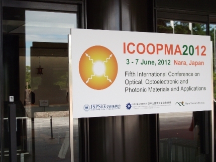
At the conference I am currently attending here in Japan (ICOOPMA 2012 – http://icoopma12.org/index.html) there is quite a lot of work being presented on Organic Light Emitting Devicess (O-LEDs) and phosphoresecent OLEDs (PhOLEDs) in addition to the stuff I am used to and was invited to present.


Of course, my immediate question was “How can something be left to be researched in a field that have been so intensively investigated during the last 15 years?”


Well… the short answer is: since there are so many LEDs around us, we need them to be more efficient in order to save energy and not devoid too fast our good old planet from its non-renewable energy resources.


The just-a-little-longer answer is: state-of-the-art LEDs located in your laptop display or mobile phone are mostly relying on fluorescence, the quantum-mechanical phenomenon involving emission of photons from singlet (spin-unpaired) quantum electronic states in Condensed Matter. Since only 25% of electrons in a solid can emit photons and light in this way, the efficiency of the device is necessarily quite poor (i.e. lower than 25%). Conversely, a complementary amount of photons (i.e. 75%) could be emitted by phosphorescence, a slower light-emission phenomenon, involving the generation of photons from from triplet (spin-paired) quantum electronic states in Condensed Matter. How to exploit phosphorescence in LEDs is still a matter of debate that is generating a lot of jobs in Condensed Matter Physics research and funds flowing from iIndistry into Academia (big flat panel display producers including Sanyo, Samsung and Toshiba are fuelling this field of research, but a lot of spin-off companies are active in this area). And, of course, since electrons and spins are involved, this is an area that is more for Applied Physicists than Engineers…. provided they have the right curriculum!


While trying to update myself on the most recent achievements in this field, I run into this very well done website I would like to share with you


http://edisontechcenter.org/LED.html


Have fun!


I could not end this post without sending a few pics from the conference venue, of course taken with a camera using a PhOLED display 😉
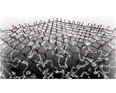
 

Dirac fermions in Molecular graphene

You can read the paper on http://www.nature.com/nature/journal/v483/n7389/fig_tab/nature10941_F1.html

MENLO PARK, US: Researchers from Stanford University and the US Department of Energy’s SLAC National Accelerator Laboratory have created the first-ever system of ‘designer electrons’- exotic variants of ordinary electrons with tunable properties that may ultimately lead to new types of materials and devices.

“The behaviour of electrons in materials is at the heart of essentially all of today’s technologies. We’re now able to tune the fundamental properties of electrons so they behave in ways rarely seen in ordinary materials,” said Hari Manoharan, Associate Professor, Stanford University.

Their first examples, reported in Nature, were hand-crafted, honeycomb-shaped structures inspired by graphene, a pure form of carbon that has been widely heralded for its potential in future electronics. Initially, the electrons in this structure had graphene-like properties; for example, unlike ordinary electrons, they had no mass and traveled as if they were moving at the speed of light in a vacuum. But researchers were then able to tune these electrons in ways that are difficult to do in real graphene.

To make the structure, which Manoharan calls molecular graphene, the scientists use a scanning tunneling microscope to place individual carbon monoxide molecules on a perfectly smooth copper surface. The carbon monoxide repels the free-flowing electrons on the copper surface and forces them into a honeycomb pattern, where they behave like graphene electrons.

To tune the electrons’ properties, the researchers repositioned the carbon monoxide molecules on the surface; this changed the symmetry of the electron flow. In some configurations, electrons acted as if they had been exposed to a magnetic or electric field. In others, researchers were able to finely tune the density of electrons on the surface by introducing defects or impurities. By writing complex patterns that mimicked changes in carbon-carbon bond lengths and strengths in graphene, the researchers were able to restore the electrons’ mass in small, selected areas.

“One of the wildest things we did was to make the electrons think they are in a huge magnetic field when, in fact, no real field had been applied,” said Manoharan. The Stanford team calculated the positions where carbon atoms in graphene should be to make its electrons believe they were being exposed to magnetic fields ranging from zero to 60 Tesla, more than 30 per cent higher than the strongest continuous magnetic field ever achieved on Earth. The researchers then moved carbon monoxide molecules to steer the electrons into precisely those positions, and the electrons responded by behaving exactly as predicted, as if they had been exposed to a real field.

“Our new approach is a powerful new test bed for physics. Molecular graphene is just the first in a series of possible designer structures. We expect that our research will ultimately identify new nanoscale materials with useful electronic properties,” said Manoharan.

Stories on carbon-based nanomaterials – Researchers create piezoelectric graphene

…The drill was using Li-doped Graphene or doping both sides of a Graphene layer with different atoms

http://www.worldofchemicals.com/media/academy/researchers-create-piezoelectri…

CALIFORNIA, US: Graphene, the most studied substance of the last decade, is one-hundred-times-better conductor of electricity than silicon. It is stronger than diamond. And, at just one atom thick, it is so thin as to be essentially a two-dimensional material. Yet, graphene is not piezoelectric. Piezoelectricity is the property of some materials to produce electric charge when bent, squeezed or twisted. Perhaps more importantly, piezoelectricity is reversible. When an electric field is applied, piezoelectric materials change shape, yielding a remarkable level of engineering control.

Piezoelectrics have found application in countless devices from watches, radios and ultrasound to the push-button starters on propane grills, but these uses all require relatively large, three-dimensional quantities of piezoelectric materials. In a paper published in the journal ACS Nano, two materials engineers at Stanford have described how they have engineered piezoelectrics into graphene, extending for the first time such fine physical control to the nanoscale.

“The physical deformations we can create are directly proportional to the electrical field applied. This represents a fundamentally new way to control electronics at the nanoscale. This phenomenon brings new dimension to the concept of ‘straintronics,’ because of the way the electrical field strains, the lattice of carbon, causing it to change shape in predictable ways,” said Evan Reed, Head of the Materials Computation and Theory Group, Stanford University.

“Piezoelectric graphene could provide an unparalleled degree of electrical, optical or mechanical control for applications ranging from touchscreens to nanoscale transistors,” said Mitchell Ong, Post-doctoral Scholar, Stanford University. Using a sophisticated modeling application running on high-performance supercomputers, the engineers simulated the deposition of atoms on one side of a graphene lattice, a process known as doping, and measured the piezoelectric effect.

They modeled graphene doped with lithium, hydrogen, potassium and fluorine, as well as combinations of hydrogen and fluorine and lithium and fluorine on either side of the lattice. Doping just one side of the graphene, or doping both sides with different atoms, is key to the process as it breaks graphene’s perfect physical symmetry, which otherwise cancels the piezoelectric effect.

“We thought the piezoelectric effect would be present, but relatively small. Yet, we were able to achieve piezoelectric levels comparable to traditional three-dimensional materials. It was pretty significant,” said Reed. The researchers were further able to fine tune the effect by pattern doping the graphene, selectively placing atoms in specific sections and not others. “We call it designer piezoelectricity because it allows us to strategically control where, when and how much the graphene is deformed by an applied electrical field with promising implications for engineering,” said Ong.

While the results in creating piezoelectric graphene are encouraging, the researchers believe that their technique might further be used to engineer piezoelectricity in nanotubes and other nanomaterials with applications ranging from electronics, photonics, and energy harvesting to chemical sensing and high-frequency acoustics. “We’re already looking at new piezoelectric devices based on other 2D and low-dimensional materials, hoping they might open new and dramatic possibilities in nanotechnology,” said Reed.

Stories on carbon-based nanomaterials – Graphene companies

Here is a list of companies involved in transfering graphene from the World of Physics into real life…

From http://www.graphene-info.com/companies

Angstron Materials

Angstron Materials logoAngstron Materials (owned by Nanotek Instruments and based in Ohio, USA) is developing and producing nano graphene platelets (NGPs), and also provide pristine graphite and single layer graphene.

In June 2011 the company announced a spin-off called Angstron Supercapacitor that will produce a new supercapacitor electrode material made from Graphene.

Angstron Materials web site

CVD Equipment

CVD logoCVD Equipment Corporation (based in Long Island, NY, USA) offers a variety of process and support equipment, for both R&D and production facilities. CVD is working together with Graphene Laboratories to offer Graphene materials and other services.

CVD’s Graphene product page


Durham Graphene Science logoDurham Graphene Science (DGS) is an R&D company that specializes in the synthesis of Graphene. The company uses a unique and scalable ‘bottom-up’ approach to prepare Graphene that is protected by a patent application. The company was founded by Dr. Karl Coleman from Durham University.

DGS’ web site

GrafTech

GrafTech logoGrafTech International is a global company with more than 120 years of experience in the carbon and graphite industry. GrafTech makes an expanded natural graphite foil that keeps most of the properties of the Graphene (thermal, electrical, and possibly acoustic) and they manufacture them in flexible sheets from 20um to 1mm thick and in widths up to about 50 inches.

GrafTech say that their graphite-foil is used in the iPhone, the new Samsung 3D TVs, and a lot of other phones and devices.

GrafTech’s web site

GRAnPH Nanotech

GRAnPH Nanotech logoGRAnPH Nanotech (based in Spain) is a provider of single-layer graphene products and other carbon based nanostructures and nanocomposites. GRAnPH developed their own patented technology for producing graphene, based on research by Grupo Antolin-Ingenieria and the Chemical Engineering Department of the University of Alicante in Spain.

The company offers its products in their on-line store.

GRAnPH Nanotech’s web site

Graphene Devices

Graphene Devices, founded in 2009 and based in Niagara Falls US is a startup that explores novel uses for Graphene and ways to optimize its production. The company is using a process developed at the University of Buffalo.

Graphene Devices has been awarded with over $600,000 in several projects in 2010 by the US federal and state authorities.

Graphene Energy

Graphene Energy logoGraphene Energy are working towards next generation nano-technology based Ultracapacitors for energy storage that will have at least twice the storage capacity of commercially available ultracapacitors. Their technology utilizes Graphene for electrode material.

Graphene Energy’s web site

Graphene Frontiers

Graphene Frontiers is a new startup established in 2011 based on new graphene-production technology developed at the University of Pennsylvania.

Graphene Frontiers’ web site

Graphene Industries

Graphene industries logo Graphene Industries is a spin-out company incorporated in March 2007 to capitalise on the advances made by Professor Andre Geim’s research group at Manchester University in the UK.

Graphene Industries is a commercial suppliers of graphene for micro- and nanoelectronic fabrication and research.

Graphene Industries web site

Graphene Laboratories

Graphene Laboratories logoGraphene Laboratories is developing and marketing functional Graphene materials and devices. The company collaborates with CVD Equipment. The company also operates the Graphene Supermarket web site which offers online graphene related products.

Graphene Labs’ web site

Graphene Supermarket

Graphene Supermarket logoGraphene Supermarket offers a broad range of graphene nanomaterials including CVD grown graphene on foils and wafers, Q-Graphene, graphene nanopowder, graphene oxide, graphene in solution, and reduced graphene oxide. Graphene Supermarket is operated by Graphene Laboratories.

You can order the Graphene production online, at Graphene Supermarket’s site.

Graphenea

Graphenea logoGraphenea is a private European company (based in Spain) focused on the production of high quality graphene for industrial applications. The company produces Monolayer Graphene Sheets, Bilayer Graphene Sheets, Multilayer Graphene Sheets, Graphene Nanosheets, Graphene Nanoplatelets and Customized Graphene.

Graphenea’s web site

Harbin Mulan Foreign Economic And Trade

Harbin Mulan, based in China and established in 2000, is engaged in the sale of carbon and graphite materials. They are providing monolayer flake graphene oxide, monolayer graphene ultra-fine powder, graphene nanoplatelets, graphene oxide membrane (thin film), graphene solution (dispersible in water, DMF solvent), carboxyl graphene, aminated graphene and thiol graphene.

Harbin Mulan’s web site

BCS: 50 YEARS

If you love History of Condensed Matter Physics you will love this book! The Scientific “Love of My Life” contribution from P W Anderson (1977 Nobel Prize for his pivotal work and understanding electron localization in amorphous materials) is simply amazing

http://www.worldscibooks.com/physics/7728.html

Edited by Leon N. Cooper & Dmitri Feldman (Brown University)

The BCS theory of superconductivity developed in 1957 by Bardeen, Cooper and Schrieffer has been remarkably successful in explaining the properties of superconductors. In addition, concepts from BCS have been incorporated into diverse fields of physics, from nuclear physics and dense quark matter to the current standard model. Practical applications include SQUIDs, magnetic resonance imaging, superconducting electronics and the transmission of electricity. This invaluable book is a compilation of both a historical account and a discussion of the current state of theory and experiment.

With contributions from many prominent scientists, it aims to introduce students and researchers to the origins, the impact and the current state of the BCS theory.


Stories on Carbon-based Nanomaterials – The Top 50 Articles on Graphene

See

http://joyinano.wordpress.com/2011/04/12/top50-articles-on-graphene/

The choice has been made on the basis of multiple parameters, including the number of citations of the articles and number of citations divided by “age” of the article. Graphene is the 2010 Nobel-award winner material.

Quite encouragingly one of our articles [Nature Nano 3 (2008) 270-274] sits at no. 38 in this top list.

Stories on Carbon-based nanomaterials – 6th Africa MRS Conference (II)

One of the reasons Zimbabwe has been chosen as a venue to the 6th Africa MRS Conference is to reconnect the local scientific community to the world after years of social and economic struggling of this Country (just a quick look on Wikipedia will help you out in understanding)

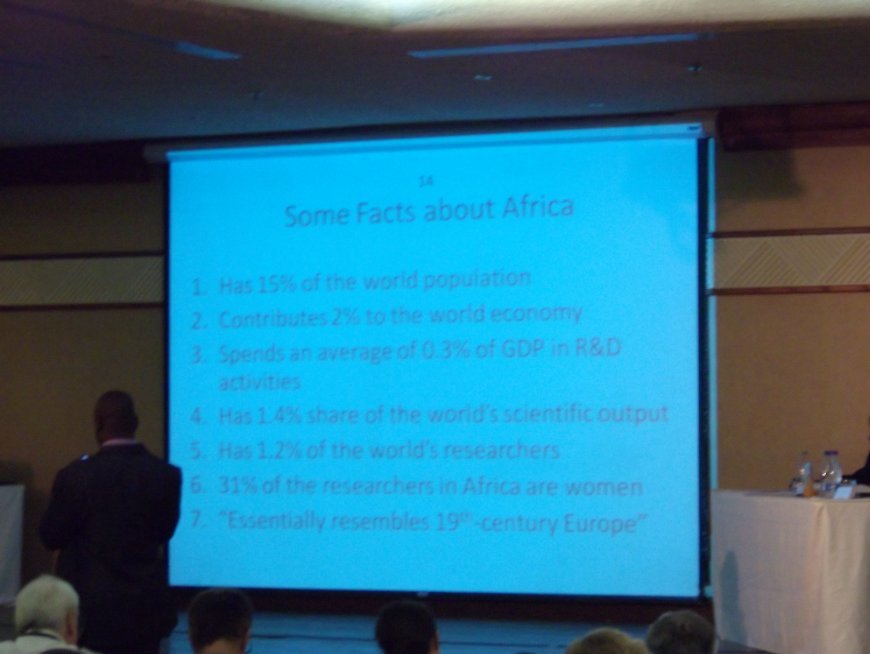
Here are a few data on Africa’s share in the World of Research I took from one slide that came out at the Plenary Session. Africa has…

  • 15% of the World population, but contributes only 2% to the World economy
  • Spends an average 0.3% GDP in R&D activities (most areas in the World are at least a few percent)
  • Has 1.4% share of the World Scientific Output
  • Has 1.2% of the World Scientific Researchers (which means an African Scientific Researcher is more productive than average, since 1.4/1.2 > 1 – We should learn from them!)
  • 31% of African researchers are Women (not sure women have the same share in Physics in Canada…)

I will keep you updated on what’s going on here!


Stories on Carbon-based nanomaterials – 6th Africa MRS Conferemce

I have been invited to present our work on Biological Properties of Graphene at the 6th Conference of the African Materials Research Society (Africa MRS).

http://www.africamrs.co.za/Home.html

Africa MRS Conferences are a great place to understand on science in developing countries and this is the main reason it is now the third time I am joining them. Symposia themes that have been chosen at the 6th Africa MRS are

  • Materials for Energy and Sustainability
  • Materials for Life, Health and the Environment
  • Basic Materials and NanoScience
  • Materials Technology, Processing and Metallurgy
  • Infrastructure Materials
  • Materials Education and Networking

So, after a 24-hr flight trip via Toronto, London UK, and Johannesburg (where I took the chance to visit some “carbon” colleagues at Wits University (www.wits.ac.za/) I am now in Zimbabwe!

The venue is great, of course. Victoria Falls are the “big sisters” of Niagara Falls, more than three times wider. this is how the Falls look like from above…

I will give my talk Tuesday afternoon and will chair the session on Graphene with African presenters I contributed to organize on Wednesday afternoon.

And here another funny spot from my hotel conference room…


Stories on Carbon-based nanomaterials

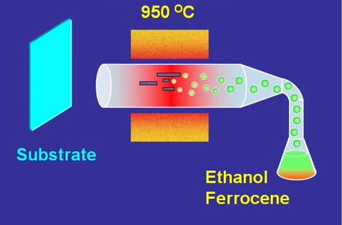
One of our methods for room temperature deposition of carbon nanotubes

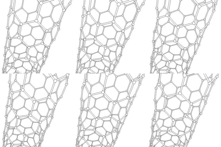
This is one of the methods we typically use fo. As many of you may know, carbon nanotubes are tubules of graphite which may have diameters less than 1 nanometer. So they are 100,000 times smaller than your hair. Ideally they should look like something like this, where every circle represents a carbon atom and every stick is a chemical bond:

Althougth it is well know that carbon nanotubes synthesize at high temperatures (typically: several hundred degree C) it is quite possible to deposit them at room temperature on virtually any tipe of substrate, making interesting transparent and conduvting networks

While what I show below is only one of many possible methods, I always find it extremely cool!!! Have fun:

Have a look at http://www.worldscinet.com/nano/05/0505/S1793292010002220.html if you are interested in more details